High Voltage Diode Full-Wave Bridge Rectifier
Full-wave rectifier design exists, and it is built around a four-diode bridge configuration. For obvious reasons, this design is called a full-wave bridge. (Figure below)

Full-wave bridge rectifier.
Current directions for the full-wave bridge rectifier circuit are as shown in Figure below for positive half-cycle and Figure below for negative half-cycles of the AC source waveform. Note that regardless of the polarity of the input, the current flows in the same direction through the load. That is, the negative half-cycle of source is a positive half-cycle at the load. The current flow is through two diodes in series for both polarities. Thus, two diode drops of the source voltage are lost (0.7·2=1.4 V for Si) in the diodes. This is a disadvantage compared with a full-wave center-tap design. This disadvantage is only a problem in very low voltage power supplies.
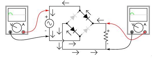
Full-wave bridge rectifier: Electron flow for positive half-cycles.
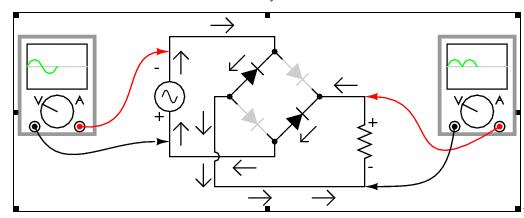
Full-wave bridge rectifier: Electron flow for negative half-cycles.
Remembering the proper layout of diodes in a full-wave bridge rectifier circuit can often be frustrating to the new student of electronics. I’ve found that an alternative representation of this circuit is easier both to remember and to comprehend. It’s the exact same circuit, except all diodes are drawn in a horizontal attitude, all “pointing” the same direction. (Figure below)

Alternative layout style for full-wave bridge rectifier.

